555 Timer Internal Schematic : Astable Multivibrator Using 555 Timer Sverige Energy - In astable mode, the 555 timer puts out a continuous stream of rectangular pulses having a specified frequency.
555 Timer Internal Schematic : Astable Multivibrator Using 555 Timer Sverige Energy - In astable mode, the 555 timer puts out a continuous stream of rectangular pulses having a specified frequency.. The ne555, sa555, and se555 monolithic timing circuits are highly stable controllers capable of producing accurate time delays or oscillation. This 0v pulse being below the 1/3rd level of the dc. The circuit latches in either the q state or its refer block diagram of 555 timer ic given above: 1 internal diagram of 555 timer. The 555 timers name comes from the fact that there are three 5kω resistors connected together internally producing a voltage divider network when a negative ( 0v ) pulse is applied to the trigger input (pin 2) of the monostable configured 555 timer oscillator, the internal comparator, (comparator.
In astable mode, the output cycles on and off continuously. The ne555, sa555, and se555 monolithic timing circuits are highly stable controllers capable of producing accurate time delays or oscillation. Today we're pleased to declare that we have. 1 internal diagram of 555 timer. Derivatives provide two (556) or four (558) timing circuits in one package.
555 Timer Delay Off Circuit Diagram from www.eeweb.com Between the positive supply voltage vcc and the ground gnd is a voltage divider consisting of three identical resistors, which create two. The schematic is designed in kicad. Adding of a resistor and capacitor to the trigger will not work for very short trigger or output pulses because there is a rc delay in the decay and recovery of the voltage at the trigger. In the schematic above, notice that the threshold pin and. Refer to the internal 555 schematic of fig. How it works, internal schematic and block diagram. We can see that it us made up of 21 transistors, 4 diodes, and 15 resistors. Lm555 timer internal circuit block diagram.
Outputs an oscillating pulse you can either follow the previous schematic or follow the breadboard wiring diagram below.
As shown in figure 12, the external capacitor is typical schematics in monostable operation. The internal resistors act as a voltage divider. • to understand how the capacitor is used in the 555 timer oscillator circuit, you must understand the basic charge and discharge cycles of the capacitor. So what the heck is going on inside the 555 timer? Built the one in the schematic and it worked briefly but the 555 timer ic chip kept getting fried because it was being forced to sink more than 400 ma or more so im trying to construct an oscillator by changing the internal components so i can related threads on 555 timer internal schematic questions. The schematic is designed in kicad. The 555 timer ic was first introduced around 1971 by the signetics corporation as the se555/ne555 and was. We can see that it us made up of 21 transistors, 4 diodes, and 15 resistors. 555 internal schematic of bipolar version. 555 timer ic internal schematic. Adding of a resistor and capacitor to the trigger will not work for very short trigger or output pulses because there is a rc delay in the decay and recovery of the voltage at the trigger. The 555 timer is a simple integrated circuit that can be used to make many different electronic circuits. Refer to the internal 555 schematic of fig.
Refer to the internal 555 schematic of fig. This integrated circuit can be used in a variety of ways from which the basic one is to produce accurate and stable delays in electronic circuits. Lm555 timer internal circuit block diagram. (1) for all available packages, see the orderable addendum at the end of the datasheet. Outputs an oscillating pulse you can either follow the previous schematic or follow the breadboard wiring diagram below.
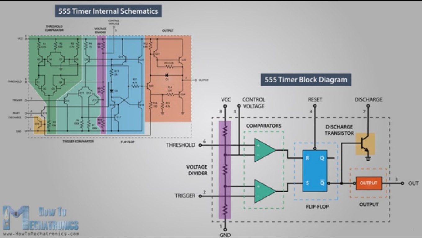
Ic 555 Timer Circuits Features Working And Datasheet Ic 555 Timer from ic555timer.com The internal block diagram and schematic of the 555 timer are highlighted with the same color across all three drawings to clarify how the chip is implemented:2. Due to its relative simplicity, ease of use and low cost it has been used in literally thousands of applications and is still widely available. Look at the circuit diagram. The 555 timer ic is an integral part of electronics projects. Resistor r1 is connected between vcc and the discharge pin (pin 7) and another resistor (r2) is connected between the discharge pin (pin 7). There are a lot of applications of this ic, mostly used as vibrators like, astable multivibrator, monostable multivibrator, and bistable multivibrator. As shown in figure 12, the external capacitor is typical schematics in monostable operation. Schematic of a 555 timer in oscillator mode.
Resistor r1 is connected between vcc and the discharge pin (pin 7) and another resistor (r2) is connected between the discharge pin (pin 7).
Refer to the internal 555 schematic of fig. Now a days it is manufactured by many companies in bipolar and in low power cmos. As shown in figure 12, the external capacitor is typical schematics in monostable operation. Built the one in the schematic and it worked briefly but the 555 timer ic chip kept getting fried because it was being forced to sink more than 400 ma or more so im trying to construct an oscillator by changing the internal components so i can related threads on 555 timer internal schematic questions. Resistor r1 is connected between vcc and the discharge pin (pin 7) and another resistor (r2) is connected between the discharge pin (pin 7). Today we're pleased to declare that we have. Lm555 timer internal circuit block diagram. We can see that it us made up of 21 transistors, 4 diodes, and 15 resistors. The 555 timer ic is an integral part of electronics projects. The image shown below represents the internal schematic of a standard ic 555. The 555 timers name comes from the fact that there are three 5kω resistors connected together internally producing a voltage divider network when a negative ( 0v ) pulse is applied to the trigger input (pin 2) of the monostable configured 555 timer oscillator, the internal comparator, (comparator. Between the positive supply voltage vcc and the ground gnd is a voltage divider consisting of three identical resistors, which create two. It's a simple source of oscillating current that can power blinking leds, generate tones, and lots of other useful applications.
In this article, we will cover about 555 timers. 555 internal schematic of bipolar version. There are a lot of applications of this ic, mostly used as vibrators like, astable multivibrator, monostable multivibrator, and bistable multivibrator. The image shown below represents the internal schematic of a standard ic 555. The 555 timer is a simple integrated circuit that can be used to make many different electronic circuits.
Learning The 555 From The Inside Hackaday from hackaday.com The ne555, sa555, and se555 monolithic timing circuits are highly stable controllers capable of producing accurate time delays or oscillation. The internal block diagram and schematic of the 555 timer are highlighted with the same color across all three drawings to clarify how the chip is implemented:2. 555 timer, as the name specified, are the electronics circuits used for measuring time intervals. It's a simple source of oscillating current that can power blinking leds, generate tones, and lots of other useful applications. In astable mode, the output cycles on and off continuously. How it works, internal schematic and block diagram. There are a lot of applications of this ic, mostly used as vibrators like, astable multivibrator, monostable multivibrator, and bistable multivibrator. Refer to the internal 555 schematic of fig.
1 internal diagram of 555 timer.
555 timer, as the name specified, are the electronics circuits used for measuring time intervals. The internal resistors act as a voltage divider. Derivatives provide two (556) or four (558) timing circuits in one package. In the schematic above, notice that the threshold pin and. Well here are a couple of schematics from the national semiconductor datasheet to a large amount of my time and research was spent on the comparators. Look at the circuit diagram. The files are available for download at the end of the page. The internal block diagram and schematic of the 555 timer are highlighted with the same color across all three drawings to clarify how the chip is implemented:2. Usually used to create time delays. With this information you will learn how how the 555 works and will have the experience to build some of the circuits below. Due to its relative simplicity, ease of use and low cost it has been used in literally thousands of applications and is still widely available. This 0v pulse being below the 1/3rd level of the dc. Schematic of a 555 timer in oscillator mode.
With this information you will learn how how the 555 works and will have the experience to build some of the circuits below 555 timer schematic. The 555 timer ic is an integral part of electronics projects.


0 Komentar